
Scanning electron microscopy (SEM)
Electron microscopy applied to radioactive materials gives insight into microscopic/ nanoscopic structures relevant for safety assessment of a nuclear repository.
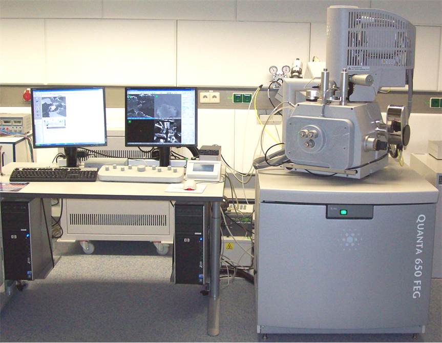
SEM analyses are performed at INE using a FEI QUANTA 650 FEG environmental scanning electron microscope located in the radioactive control area (Fig. 1). In SEM, a fine electron probe is focussed on the surface of a sample and scanned in a two-dimensional raster. At each point, various emitted signals can be detected and contribute to a corresponding point in an image. So-called secondary electrons (SE) enable the observation of surface topography with a lateral resolution down to few nanometers, whereas images produced by means of elastically backscattered electrons (BSE) present an elemental contrast. Furthermore, the detection of characteristic x-rays allows quantitative determination of atomic concentrations at a micrometer scale (energy-dispersive x-ray spectroscopy, EDX).
Contact:
+49 721 608 22521 / 22379
+49 721 608 24602